- 您现在的位置:买卖IC网 > Sheet目录3890 > PIC18C858T-E/PT (Microchip Technology)IC MCU OTP 16KX16 CAN 80TQFP
PIC18CXX8
DS30475A-page 100
Advanced Information
2000 Microchip Technology Inc.
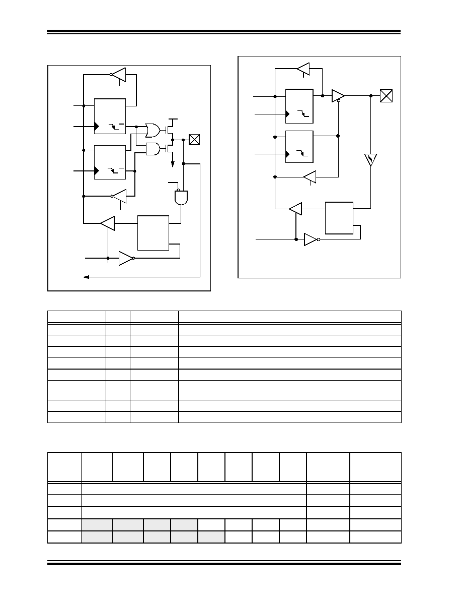
FIGURE 8-10: RF6:RF3 AND RF0 PINS
BLOCK DIAGRAM
FIGURE 8-11: RF7 PIN BLOCK DIAGRAM
TABLE 8-11:
PORTF FUNCTIONS
TABLE 8-12:
SUMMARY OF REGISTERS ASSOCIATED WITH PORTF
Data
Bus
Q
D
Q
CK
Q
D
Q
CK
QD
EN
P
N
WR LATF
WR TRISF
Data Latch
TRIS Latch
RD TRISF
RD PORTF
VSS
VDD
I/O Pin
Analog
Input
Mode
ST
Input
Buffer
To A/D Converter or Comparator Input
RD LATF
or
WR PORTF
Note:
I/O pins have diode protection to VDD and VSS.
Data
Bus
WR LATF
WR TRISF
RD PORTF
Data Latch
TRIS Latch
RD TRISF
Schmitt
Trigger
Input
Buffer
I/O pin
Q
D
CK
Q
D
CK
EN
QD
EN
RD LATF
or
WR PORTF
Note:
I/O pins have diode protection to VDD and VSS.
Name
Bit#
Buffer Type
Function
RF0/AN5
bit0
ST
Input/output port pin or analog input.
RF1/AN6/C2OUT
bit1
ST
Input/output port pin or analog input or comparator 2 output.
RF2/AN7/C1OUT
bit2
ST
Input/output port pin or analog input or comparator 1 output.
RF3/AN8
bit3
ST
Input/output port pin or analog input or comparator input.
RF4/AN9
bit4
ST
Input/output port pin or analog input or comparator input.
RF5/AN10/
CVREF
bit5
ST
Input/output port pin or analog input or comparator input or comparator
reference output.
RF6/AN11
bit6
ST
Input/output port pin or analog input or comparator input.
RF7
bit7
ST
Input/output port pin.
Legend: ST = Schmitt Trigger input
Name
Bit 7
Bit 6
Bit 5
Bit 4
Bit 3
Bit 2
Bit 1
Bit 0
Value on:
POR,
BOR
Value on all
other RESETS
TRISF
PORTF Data Direction Control Register
1111 1111
PORTF
Read PORTF pin / Write PORTF Data Latch
xxxx xxxx
uuuu uuuu
LATF
Read PORTF Data Latch/Write PORTF Data Latch
0000 0000
uuuu uuuu
ADCON1
—
VCFG1 VCFG0 PCFG3 PCFG2 PCFG1 PCFG0 --00 0000
--00 0000
CMCON
C2OUT
C1OUT
C2INV
C1INV
CIS
CM2
CM1
CM0
0000 0000
Legend: x = unknown, u = unchanged
发布紧急采购,3分钟左右您将得到回复。
相关PDF资料
PIC18C858T-I/PT
IC MCU OTP 16KX16 CAN 80TQFP
PIC18C658T-I/PT
IC MCU OTP 16KX16 CAN 64TQFP
PIC16LC717T-E/SS
IC MCU OTP 2KX14 A/D PWM 20SSOP
PIC16LC771T/SO
IC MCU OTP 4KX14 A/D PWM 20SOIC
PIC16LC771T-E/SO
IC MCU OTP 4KX14 A/D PWM 20SOIC
PIC16C771T-E/SO
IC MCU OTP 4KX14 A/D PWM 20SOIC
PIC16LC770T/SS
IC MCU OTP 2KX14 A/D PWM 20SSOP
PIC16LC717T-I/SO
IC MCU OTP 2KX14 A/D PWM 18SOIC
相关代理商/技术参数
PIC18C858T-I/L
功能描述:8位微控制器 -MCU 40MHz 16K OTP RoHS:否 制造商:Silicon Labs 核心:8051 处理器系列:C8051F39x 数据总线宽度:8 bit 最大时钟频率:50 MHz 程序存储器大小:16 KB 数据 RAM 大小:1 KB 片上 ADC:Yes 工作电源电压:1.8 V to 3.6 V 工作温度范围:- 40 C to + 105 C 封装 / 箱体:QFN-20 安装风格:SMD/SMT
PIC18C858T-I/PT
功能描述:8位微控制器 -MCU 32KB 1536 RAM 68I/O RoHS:否 制造商:Silicon Labs 核心:8051 处理器系列:C8051F39x 数据总线宽度:8 bit 最大时钟频率:50 MHz 程序存储器大小:16 KB 数据 RAM 大小:1 KB 片上 ADC:Yes 工作电源电压:1.8 V to 3.6 V 工作温度范围:- 40 C to + 105 C 封装 / 箱体:QFN-20 安装风格:SMD/SMT
PIC18F1220-E/ML
功能描述:8位微控制器 -MCU 4KB 256 RAM 16 I/O RoHS:否 制造商:Silicon Labs 核心:8051 处理器系列:C8051F39x 数据总线宽度:8 bit 最大时钟频率:50 MHz 程序存储器大小:16 KB 数据 RAM 大小:1 KB 片上 ADC:Yes 工作电源电压:1.8 V to 3.6 V 工作温度范围:- 40 C to + 105 C 封装 / 箱体:QFN-20 安装风格:SMD/SMT
PIC18F1220-E/P
功能描述:8位微控制器 -MCU 4KB 256 RAM 16 I/O RoHS:否 制造商:Silicon Labs 核心:8051 处理器系列:C8051F39x 数据总线宽度:8 bit 最大时钟频率:50 MHz 程序存储器大小:16 KB 数据 RAM 大小:1 KB 片上 ADC:Yes 工作电源电压:1.8 V to 3.6 V 工作温度范围:- 40 C to + 105 C 封装 / 箱体:QFN-20 安装风格:SMD/SMT
PIC18F1220-E/SO
功能描述:8位微控制器 -MCU 4KB 256 RAM 16 I/O RoHS:否 制造商:Silicon Labs 核心:8051 处理器系列:C8051F39x 数据总线宽度:8 bit 最大时钟频率:50 MHz 程序存储器大小:16 KB 数据 RAM 大小:1 KB 片上 ADC:Yes 工作电源电压:1.8 V to 3.6 V 工作温度范围:- 40 C to + 105 C 封装 / 箱体:QFN-20 安装风格:SMD/SMT
PIC18F1220-E/SS
功能描述:8位微控制器 -MCU 4KB 256 RAM 16 I/O RoHS:否 制造商:Silicon Labs 核心:8051 处理器系列:C8051F39x 数据总线宽度:8 bit 最大时钟频率:50 MHz 程序存储器大小:16 KB 数据 RAM 大小:1 KB 片上 ADC:Yes 工作电源电压:1.8 V to 3.6 V 工作温度范围:- 40 C to + 105 C 封装 / 箱体:QFN-20 安装风格:SMD/SMT
PIC18F1220-H/ML
功能描述:8位微控制器 -MCU 4KB FL 256RAM 16 I/O RoHS:否 制造商:Silicon Labs 核心:8051 处理器系列:C8051F39x 数据总线宽度:8 bit 最大时钟频率:50 MHz 程序存储器大小:16 KB 数据 RAM 大小:1 KB 片上 ADC:Yes 工作电源电压:1.8 V to 3.6 V 工作温度范围:- 40 C to + 105 C 封装 / 箱体:QFN-20 安装风格:SMD/SMT
PIC18F1220-H/P
功能描述:8位微控制器 -MCU 4KB FL 256RAM 16 I/O RoHS:否 制造商:Silicon Labs 核心:8051 处理器系列:C8051F39x 数据总线宽度:8 bit 最大时钟频率:50 MHz 程序存储器大小:16 KB 数据 RAM 大小:1 KB 片上 ADC:Yes 工作电源电压:1.8 V to 3.6 V 工作温度范围:- 40 C to + 105 C 封装 / 箱体:QFN-20 安装风格:SMD/SMT